UCLA physicists map atoms in 3D

Have you ever tried those magical pieces of software that merge multiple pictures of an object from different angles to produce a 3D model of it?

Good. Now think about upgrading your equipment, because those guys at UCLA do the same with atoms. Seriously.

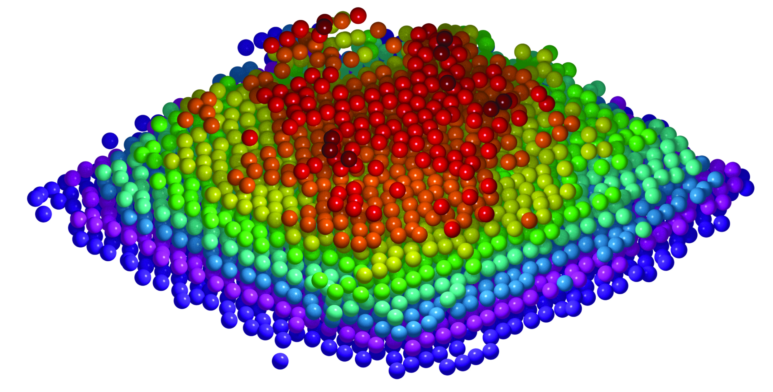
Using a scanning transmission electron microscope at the Lawrence Berkeley National Laboratory’s Molecular Foundry, Miao and his colleagues analyzed a small piece of tungsten, an element used in incandescent light bulbs. As the sample was tilted 62 times, the researchers were able to slowly assemble a 3-D model of 3,769 atoms in the tip of the tungsten sample.

Here’s the final result

The 3-D coordinates of thousands of individual atoms and a point defect in a material were determined with a precision of 19 trillionths of a meter, where the crystallinity of the material is not assumed. The figure shows the measured 3-D atomic positions of a tungsten tip, consisting of nine atomic layers, labelled with crimson (dark red), red, orange, yellow, green, cyan, blue, magenta and purple from layers one (top) to nine (bottom), respectively.


Original article here.